Stm32f429zi stm32f4discovery: Difference between revisions
Created STM32F429 discovery page |
updated code uploading guide |
||
| (One intermediate revision by the same user not shown) | |||
| Line 5: | Line 5: | ||
* An external 64Mb SRAM, L3GD20 3-axis digital output gyroscope, 2.4" QVGA TFT LCD, 2 user LEDs, user button, reset button, a second USB connector as the microcontroller supports USB. | * An external 64Mb SRAM, L3GD20 3-axis digital output gyroscope, 2.4" QVGA TFT LCD, 2 user LEDs, user button, reset button, a second USB connector as the microcontroller supports USB. | ||
[[File: | [[File:Stm32f429disco.jpg|frameless]] | ||
== Configuring the kernel == | == Configuring the kernel == | ||
| Line 55: | Line 55: | ||
As explained before, there are more than one linker script for this board, and the selected linker script affects the way code should be loaded on the board. | As explained before, there are more than one linker script for this board, and the selected linker script affects the way code should be loaded on the board. | ||
A simple way to load code in FLASH is to use the [https://github.com/fpoussin/QStlink2 QStlink2] tool. Also, if you have a brand new board and QStlink fails you may take a look at [[ST-LINK utility update|this page]] | |||
== Reading printf output == | == Reading printf output == | ||
Latest revision as of 08:42, 16 December 2016
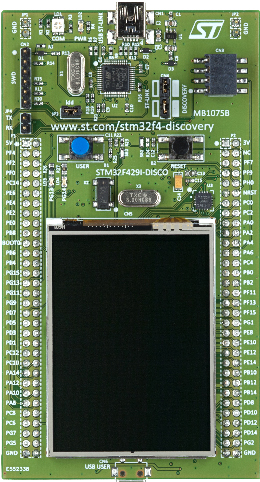
This is a cheap self contained discovery board with a powerful processor, and a Linux-friendly ST-LINK/V2 programmer/in circuit debugger. The board is equipped with
- A STM32F429ZI microcontroller with a 180MHz ARM Cortex-M4F core, 2048KB Flash, 256KB RAM, 4KB battery-backed RAM in LQFP144 package.
- An external 64Mb SRAM, L3GD20 3-axis digital output gyroscope, 2.4" QVGA TFT LCD, 2 user LEDs, user button, reset button, a second USB connector as the microcontroller supports USB.
Configuring the kernel
The minimum configuration required is to edit the miosix/config/Makefile.inc file to uncomment the OPT_BOARD := stm32f429zi_stm32f4discovery line. If you had compiled the kernel before, it is recommended to do a make clean (or in the Netbeans IDE, to click on the "Clean project" button) to avoid leaving object files around. After, do a make to compile.
In addition, this board has a couple of board-specific options in the Makefile.inc file. For convenience, the relevant part of that configuration file is reported here so as to be easily located within the file
##---------------------------------------------------------------------------
## stm32f429zi_stm32f4discovery
##
ifeq ($(OPT_BOARD),stm32f429zi_stm32f4discovery)

    ## Linker script type, there are three options
    ## 1) Code in FLASH, stack + heap in internal RAM (file *_rom.ld)
    ##    the most common choice, available for all microcontrollers
    ## 2) Code in FLASH, stack + heap in external RAM (file *8m_xram.ld)
    ##    You must uncomment -D__ENABLE_XRAM below in this case.
    ## 3) Code in FLASH, stack + heap in external RAM (file *6m_xram.ld)
    ##    Same as above, but leaves the upper 2MB of RAM for the LCD.
    LINKER_SCRIPT_PATH := arch/cortexM4_stm32f4/stm32f429zi_stm32f4discovery/
    #LINKER_SCRIPT := $(LINKER_SCRIPT_PATH)stm32_2m+256k_rom.ld
    #LINKER_SCRIPT := $(LINKER_SCRIPT_PATH)stm32_2m+8m_xram.ld
    LINKER_SCRIPT := $(LINKER_SCRIPT_PATH)stm32_2m+6m_xram.ld

    ## Uncommenting __ENABLE_XRAM enables the initialization of the external
    ## 8MB SDRAM memory. Do not uncomment this even if you don't use a linker
    ## script that requires it, as it is used for the LCD framebuffer.
    XRAM := -D__ENABLE_XRAM

    ## Select clock frequency. Warning: the default clock frequency for
    ## this board is 168MHz and not 180MHz because, due to a limitation in
    ## the PLL, it is not possible to generate a precise 48MHz output when
    ## running the core at 180MHz. If 180MHz is chosen the USB peripheral will
    ## NOT WORK and the SDIO and RNG will run ~6% slower (45MHz insteand of 48)
    #CLOCK_FREQ := -DHSE_VALUE=8000000 -DSYSCLK_FREQ_180MHz=180000000
    CLOCK_FREQ := -DHSE_VALUE=8000000 -DSYSCLK_FREQ_168MHz=168000000
    #CLOCK_FREQ := -DHSE_VALUE=8000000 -DSYSCLK_FREQ_100MHz=100000000

endif
As can be seen, there are two options for this board: LINKER_SCRIPT and SRAM_BOOT. The comments explain in detail the meaning of there options, so it isn't necessary to further explain them.
After modifying configuration files it is recommended to do a make clean; make (or in the Netbeans IDE, to click on the "Clean and build project" button) to be sure that changes are applied.
Loading code
As explained before, there are more than one linker script for this board, and the selected linker script affects the way code should be loaded on the board.
A simple way to load code in FLASH is to use the QStlink2 tool. Also, if you have a brand new board and QStlink fails you may take a look at this page
Reading printf output
The board has no serial to USB adapter onboard, so you need to use an external one, connected to USART3, in detail PA9 (TXD) and PA10 (RXD).
On Linux you can use screen. Open a terminal and type screen /dev/ttyUSB0 19200 (Note that to quit from screen you need to type "Ctrl-C, \"). You'll need to change /dev/ttyUSB0 with your serial port device name.
On windows you can use HyperTerminal, you need to configure it to use the required baud rate, no flow control, and select the correct COM port device name.
In Circuit Debugging
Before you begin you should note that the Miosix kernel will put the CPU to a low power state when no thread is running. This low power state will usually confuse debuggers and make them lose sync with the CPU. To avoid this you need to edit the miosix/config/miosix_settings.h file and uncomment #define JTAG_DISABLE_SLEEP line. This will prevent the kernel from putting the CPU in its low power state making debugging possible. Also, to be able to precisely single-step your code you need to disable compiler optimizations as gdb is incapable of reliably debug an optimized code. The option is in the miosix/config/Makefile.inc file and is the OPT_OPTIMIZATION := -O0 that should be uncommented while the other lines related to the same option should be commented out.
After modifying configuration files it is recommended to do a make clean; make (or in the Netbeans IDE, to click on the "Clean and build project" button) to be sure that changes are applied.
Since the board has an on board SWD in circuit debugger, simply plugging the USB cable is all you need from an hardware point of view. On the software side, you need to open two shells. In one do a
sudo openocd -f miosix/arch/cortexM4_stm32f4/stm32f429zi_stm32f4discovery/stm32f4discovery.cfg
This will start the OpenOCD program that will connect to the board and listen for GDB connections.
In the second shell type the following commands
arm-miosix-eabi-gdb main.elf
target remote :3333
monitor soft_reset_halt
break main
continue
The first command will start the gdb debugger. The following commands are typed into the gdb console, and tell it to connect to OpenOCD, and reset the board and stop the program at the beginning of main() To load the program to be debugged, you can either do a make program before and then start debugging, or you can directly write the FLASH memory from within gdb with this command
monitor flash write_image erase main.bin 0x08000000
From there on, have a look at Quick_start for debugger commands.
(Optional) Configuring the Netbeans IDE
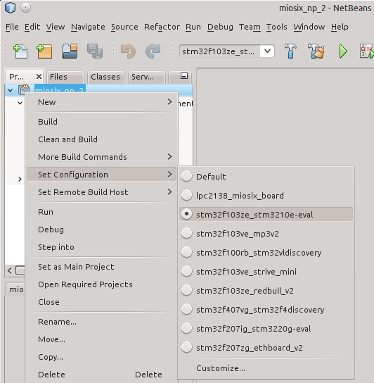
To have a fully working code completion that can also resolve the board-specific symbols, right click on the project, go to Set Configuration and select the right board.
SD Card (FIXME!!!!)
This board lacks an SD connector, so the filesystem support does not work out of the box (upon boot the kernel will say that filesystem mounting failed). However, it is possible to connect one to specific GPIO pins.
The SD or microSD connector VCC and GND pins need to be connected to 3V and GND pins on the board. Add a 100nF capacitor between VCC and GND, as close as possible to the SD connector. This will be useful to overcome current absorption peaks from the SD card.
Then connect the following GPIOs to the SD connector.
| SD | STM32 | Optional |
|---|---|---|
| CLK | PC12 | |
| CMD | PD2 | |
| D0 | PC8 | |
| D1 | PC9 | Y |
| D2 | PC10 | Y |
| D3 | PC11 | Y |
Each connection needs a pullup resistor between ~47Kohm and 100Kohm.
To increase read/write speed it is possible to connect the optional GPIOs thereby communicating with the SD in 4-bit mode. Note that by default in this board the SD driver uses 1 bit mode. To enable 4-bit mode you need to edit the miosix/config/arch/cortexM4_stm32f4/stm32f407vg_stm32f4discovery/board_settings.h and comment out the #define SD_ONE_BIT_DATABUS line.
Also note that filesystem support is enabled by default, so the pins marked as not optional are used by the filesystem driver. If you do not want to connect an SD card, and want to use those GPIOs, you should disable the filesystem support in miosix/config/miosix_settings.h.
Resource
stm32f4discovery Datasheet

