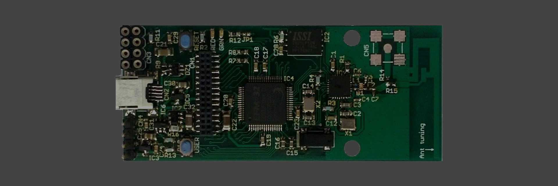
High-performance MCU
Thanks to its powerful ARM Cortex-M3 core running at up to 48MHz, WandStem is capable of complex on-node sensor post-processing, from filtering to Fourier transforms.
The microcontroller at the heart of WandStem has on-chip 1MB flash and 128KB RAM. This is the largest available memory currently available in an ultra low power node. The ample RAM allows large data buffers for sensor data, and big routing tables for dense networks. The large flash can instead be used to store software libraries to program at a higher abstraction level. Finally, an off-chip 16MB flash is available through a filesystem API for long-term data and configuration files storage.
Miosix operating system
WandStem is powered by the Miosix OS, a versatile operating system for embedded devices. Compared to alternatives, which often require to learn a domain-specific language, or use a restricted subset of C, Miosix application development is done using standard C++, including its standard libraries such as the STL. Moreover, the kernel features preemptive multitasking using the standard PTHREAD API. This lowers the learning curve for developing applications and enables the development of real-time applications.
Ultra-low power consumption
In IoT and cyber-phisical applications having a powerful node is not useful if batteries have to be replaced very often.
The WandStem node features best in class deep-sleep consumption, down to 2.4μA, enabling years of continuous operation.
This consumption figure is for the entire node, including retention of the full 128KB of SRAM, and with the RTC running from the external crystal oscillator. The first feature is important as it allows deep sleep to be transparent to applications, while the second makes timekeeping in deep sleep possible, as well as time triggered wakeups.
Hardware accelarated timing
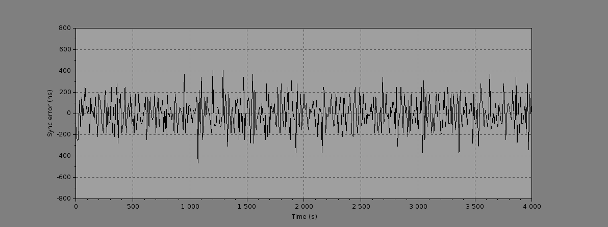
The WandStem node has been engineered from the beginning to achieve the best possible clock synchronization accuracy. The node is capable of keeping track of time with a 21ns resolution, and a 64 bit time representation.
WandStem is the first node supporting hardware timed packet transmission, so you can ask the radio stack to send a packet at a precise point in time, with 21ns resolution, and without software induced jitter. Of course, WandStem also supports hardware packet timestamping to know precisely when incoming packets have been received.
Hardware support is also included to implement the VHT algorithm so as to preserve the high resolution time representation across deep-sleep periods.
Skew and drift compensation
Having good timestamping is not enough for an accurate time synchronization. Each node in the network has a clock crystal with its own slightly different frequency, causing clock skew to accumulate. Did you know that an average crystal can accumulate an error of more than 1.5 milliseconds per minute? Moreover, temperature chenges affect the crystal oscillation frequency, making it a time-varying value. This phenomenon is called clock drift.
WandStem employs the FLOPSYNC-2 scheme an approach grounded on control theory that compensates for both clock skew and drift. This provides an enhancement compared to previous approaches, e.g. using linear regression, which only compensate for skew.
Propagation delay compensation
WandStem uses the Glossy flooding protocol to minimize jitter accumulation in a multi-hop network. However, propagation delays can still introduce a noticeable synchronization error in large networks.
To compensate for that, WandStem uses the Reverse flooding scheme, a technique that can measure, and thus compensate for, the propagation delay of flooded time packets. As a result, sub-microsecond clock synchronization is achievable also for networks that span more than 300 meters.
Onboard current sensor
The toughest requirement in battery operated devices is achieving the desired preformance within the available energy budget. WandStem is the first node providing an on-board current sensor
to monitor the node consumption, both during the development and deployment phase.
This hardware feature allows to discover energy affecting software bugs such as missed opportunities to go to deep sleep, that would otherwise go unnoticed.
To always know how much energy is left in the batteries, the current sensor enables Coulomb counting, thus having a reliable battery meter also with lithium batteries. An innovative off-line model allows to account for deep-sleep energy consumption without increasing deep-sleep current.
Interfacing
Interfacing WandStem with sensors is performed through shields attached through and expansion connector. GPIOs, SPI, I²C, USART, ADC, DAC, PWM, we've got them all. The expansion connector features the output of a dedicated power switch to turn off power hungry sensors when not used. Battery charging shields are also possible, e.g. for energy harvesting.
The microcontroller has USB device and host hardware, thus allowing easy interfacing to a PC for fast data exchange. When the USB cable is connected, a second power switch disconnects the batteries to extend their life. Programming the node is done through an USB bootloader.
Want buttons and LEDs? Sure, we have them too.
Standard IEEE 802.15.4 radio
WandStem uses the industry-standard IEEE 802.15.4 radio protocol, operating in the 2.4GHz frequency band with 16 channles, and a data rate of 250Kbps. The node features the widely known cc2520 radio transceiver.
When coupled with the highly accurate time synchronization, advanced protocols making use of channel hopping, constructive interference, TDMA and bandwidth assignment are possible.
Contact us
We are currently doing a pre production batch of nodes, for information on the node availability and pricing, send an email to  .
.
Download the open version
The schematic files of WandStem Open can be downloaded as Open Hardware, released under a creative commons CC-BY-SA license.
WandStem rev 1.3A: the latest version.
WandStem rev 1.3
WandStem rev 1.0
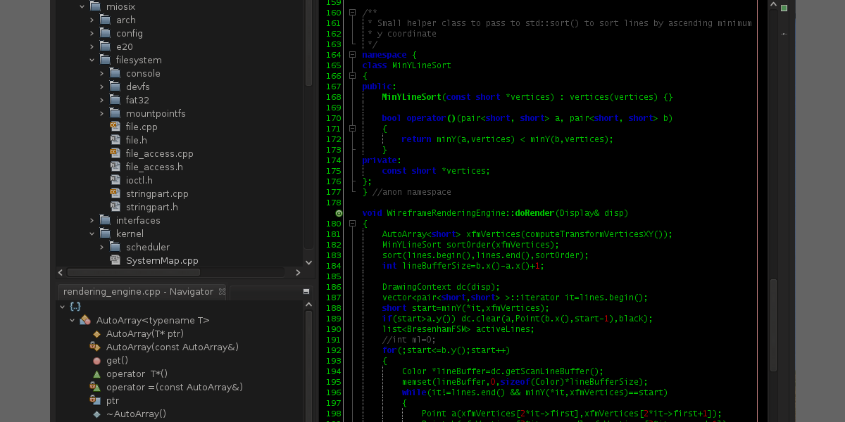
The Miosix kernel is available here, the WandStem board support package is already available in the testing branch. Additional code is available in the flopsync codebase, and is currently being merged in the kernel.